Microchip is undeniably the greatest invention of humankind since the end of the Atomic Era. It has been the fuel for the current Information Era, the backbone of modern technology, and is now everywhere in the daily life of people. Most of us have seen the image of a microchip: a little black square with a size slightly larger than a coin that sits silently in the corner of our laptops, PCs, or smartphones. But few have ever seen the very inside of these black boxes, where a whole city of glass and metal was built, a miraculous feat of engineering that realizes the idea of “given enough Ifs, I can put the whole Paris in a bottle”.
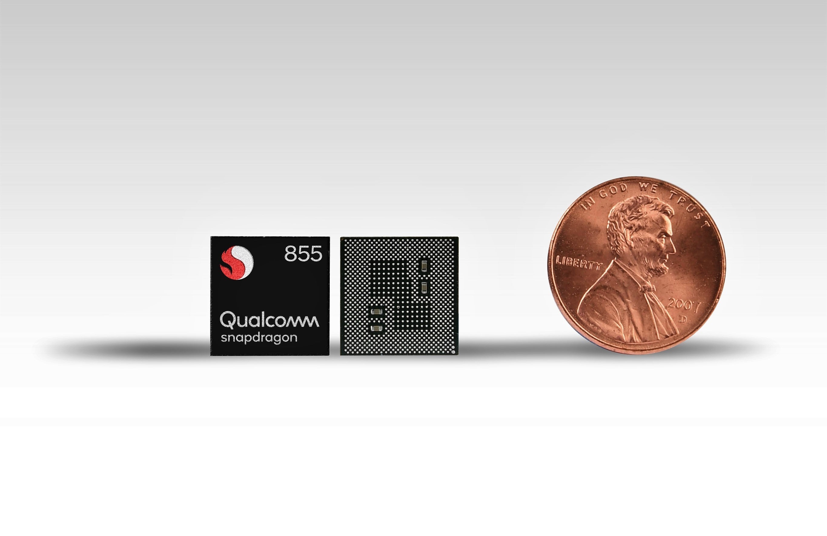
I am an engineer at Qualcomm – the company that made that little Snapdragon 855 you see in the above picture (Fig.1). My daily work is to perform surgery on the dead bodies of unfortunate microchips, those who did not survive the production process, or were killed when being used by “cruel” users. And just like in CSI: Miami, I’m a member of the Forensic team who would open up these corpses, look into their organs & skins & bones, and try to find out the reason of death. Join me in one of these surgery sessions, where you get to see a microchip in the way you’ve never seen before, demystifying all questions you used to have on those mysterious black boxes.
DECAPSULATION
Microchips came in different sizes, shapes, and packages. However, their structure is basically the same. In the below picture (Fig.2), you can have a brief idea of what is inside the chip as the surgeon started to open up its body and reveal its organs – a process we called decapsulation. Inside that black box, positioned in the center of everything, is the silicon die, the most sacred, important part of the whole chip. If compare the microchip to a human body, then the silicon die is definitely the brain, a super big brain that takes up almost all the space, which makes sense since all the chip ever does is computing.
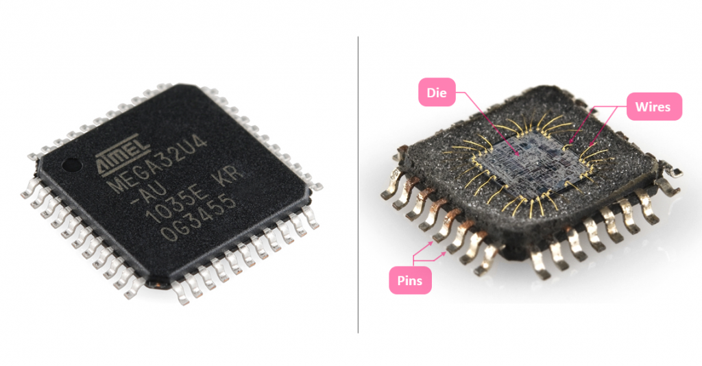
Besides being very important, the die is also extremely fragile (silicon is actually glass), and therefore must be protected by wrapping around it a plastic resin – called mold compound. This compound is the black material that you see embracing the die and wires, keeping them safe inside an enclosed capsule (now you see why opening it up is called de-capsulation). Of course, it cannot fully enshroud the die – there must be a way for the die to make contact with the outside world. And that connection is made using bonding wires – each one connects from the die to a pin outside. These bonding wires are previously made of actual gold – some Youtubers really go collect these thrown away devices and extract the gold from them, though it requires professional chemistry level. The outside pins will later be soldered into the motherboard – spreading electrical signals from the die to the other devices.
SILICON DIE
Now comes the exciting part – to investigate the silicon die. After carefully removing the die from its protective mold compound, we placed it under the microscope and take a look – as in below Fig.3-left is showing you (you can still see the aforementioned bonding wires attached to several pads along the borders).
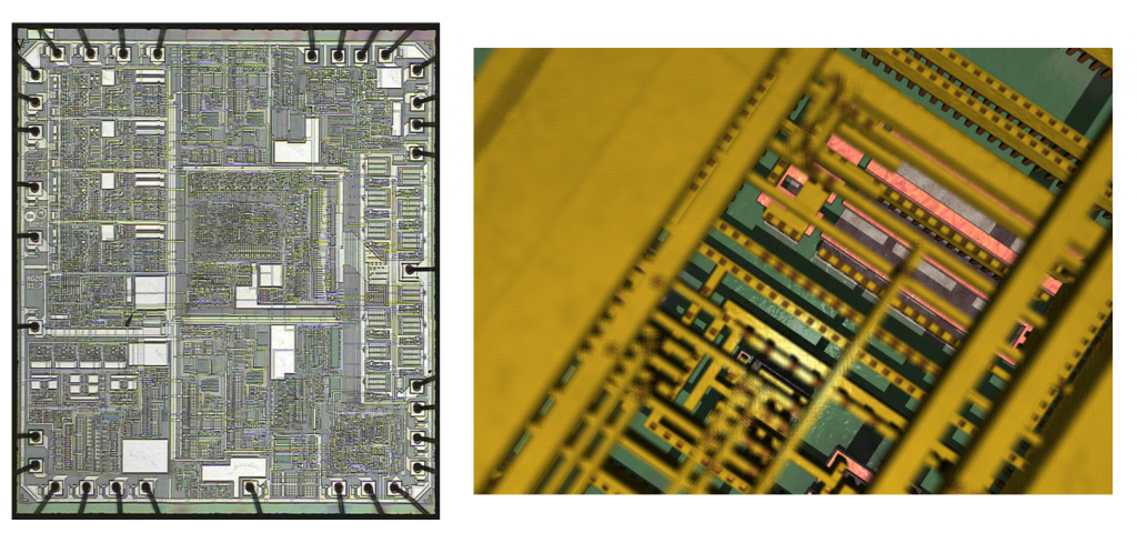
If the black microchip is already very small, this die is even smaller, and thinner. There are reasons as to why the silicon die becomes the most valuable component in the chip, the most simple and straightforward to be – it is incredibly complex. Despite its tiny size, the die is literally a city with houses & buildings made of transistors, connecting together by streets of copper and highways of aluminum creating multiple layers of metal. The latest microprocessors often consist of more than 10 metal layers, each one stacking on top of each other and are connected together using metal vias. This system of metal lines and cylindrical contacts is called layers of interconnects.
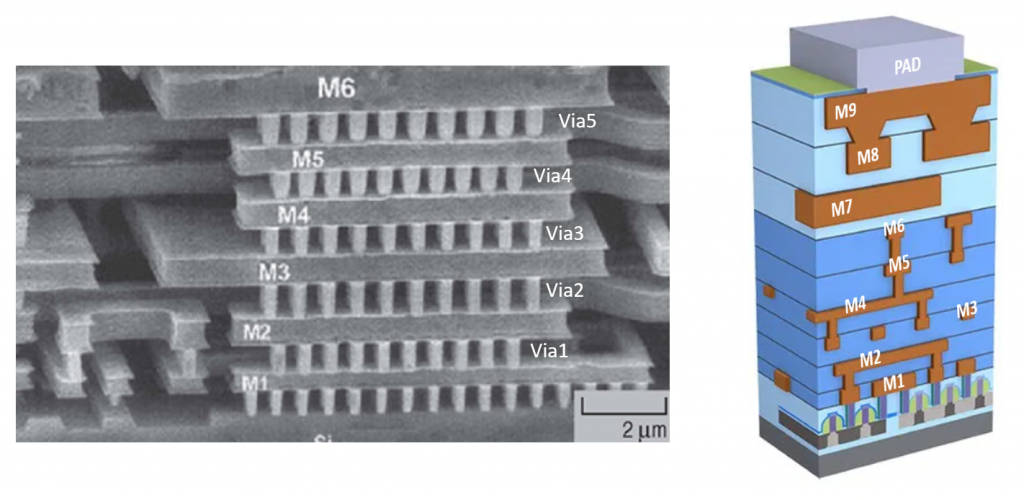
A bird-eye view is presented to you in Fig.3-right. You can see different levels of metal traces crossing each other with more blurry layers on top. The 3D images below (Fig.4) describe how these metal layers are stacked up and numbered accordingly.
Below all these metal traces and vias are the layer of the famous transistors. While the metal traces only help in connection, transistors are the main components that actually compute. These transistors are similar to neurons in human brains. Even though each one of them basically just controls a single 0 or 1 value (called boolean value), its strength lies in the massive numbers. The latest Apple A13 Bionic consists of around 8.5 billion transistors [1], more than the population of current Earth. And to be able to pack billions of transistors on an area slightly larger than a fingernail, each one of them has to be shrunk to the size of a 10 – 20 nanometer wide. How small is that? Small enough to pack more than one-thousand transistors across the diameter-of-your-hair. This struggle to shrink transistor size has been going on for decades, with every 2 years the chipmakers have been able to make them two times smaller than before, a journey that is often known to us as Moore’s law [2].
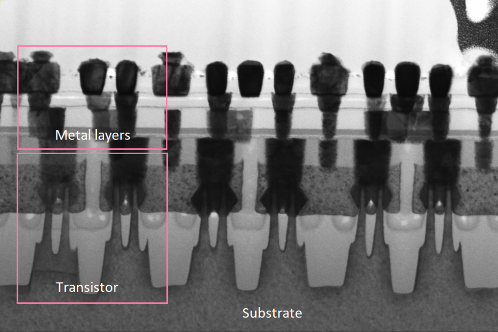
Finally, below the transistor level is a thick layer of silicon, which is called substrate. This layer contains all the doping necessary to make the transistors active. The material for substrate must always be semiconductor – able to switch between conducting and non-conducting states – enabling the transistor to represent a binary value of either 0 or 1. Almost every current microchip is using silicon (Si) as its substrate element, due to its efficiency and remarkably low-cost. The silicon was manufactured from sand, not the one that can be found from beaches, but silica sand which people usually get from quarrying [3]. This high-quality sand will later be refined into pure Silicon with an exceptional low level of foreign particles, and then be used in foundries to create the substrate for microchips.
And that is brief anatomy of what is inside a microchip. To finalize this article below is some fancy video footage from Intel on how microchips are made. The technology in the clip is 22nm, which is a few years back, but its visual illustration is still very interesting and useful to grab an idea of how this Paris in a bottle was created.
Reference:
- Jason Cross, “Inside Apple’s A13 Bionic system-on-chip”. Available: Macworld.
- Moore GE (1965) Cramming more components onto integrated circuits. Electronics 38(6).
- Carrie Marshall (August 25, 2016), “From sandy beach to Kaby Lake: How sand becomes silicon”.
First of all I would like to say excellent blog! I had a quick question in which I’d like to ask if you do not mind.
I was interested to find out how you center yourself and clear your mind prior to writing.
I have had a tough time clearing my mind in getting my ideas out there.
I do take pleasure in writing but it just seems like the first 10
to 15 minutes are usually wasted simply just trying to figure out how to begin. Any suggestions or hints?
Cheers!
Hmm it seems like your site ate my first comment (it was extremely long) so I guess I’ll just
sum it up what I had written and say, I’m thoroughly enjoying your
blog. I too am an aspiring blog writer but I’m
still new to the whole thing. Do you have any recommendations for beginner blog writers?
I’d definitely appreciate it.
You can start writing about things that related to your study & work, that the more you research, the more it benefits you.
Make a framework of what you’re going to write, what’s the whole article is about and how many parts there are gonna be.
Use Grammarly to aid you in English writing.
Thank you and wish you all the best!
Hello there! This blog post couldn’t be
written much better! Looking at this post reminds me of my previous roommate!
He continually kept talking about this. I most certainly will send this post to him.
Fairly certain he’s going to have a very good read. I appreciate you for sharing!
You’ve made some good points there. I looked on the web
for additional information about the issue and found most individuals will go along with your
views on this website.
I love your blog.. very nice colors & theme.
Did you design this website yourself or did you hire someone to do it for you?
Plz respond as I’m looking to design my own blog
and would like to find out where u got this from. many thanks
I used a plugin called Elementor, which is very helpful and convenient!
Howdy! I realize this is kind of off-topic but I had to ask.
Does operating a well-established website such as yours require a lot of work?
I am completely new to writing a blog but I do write in my journal every day.
I’d like to start a blog so I can share my personal
experience and views online. Please let me know if you have any kind of ideas or tips
for brand new aspiring blog owners. Appreciate it!
Really informative blog.Thanks Again.
Fine way of explaining, and pleasant piece of
writing to obtain facts on the topic of my presentation subject matter, which i am going to present
in university.