In late 2020, when the whole world is still struggling in the worst pandemic ever since the Spanish flu, another storm is churning up in the semiconductor industry and would be quick to spread over the globe just like the way COVID-19 did. The world is now facing a global chip shortage, a phenomenon that may brutally damage the post-pandemic recovery efforts of many companies and countries. Every industry from tech giants to carmakers and suppliers of consumer goods is feeling the heavy impact of this hit.
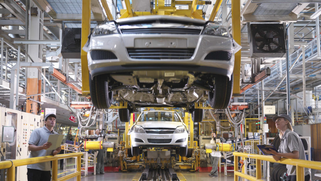
“If software is eating the world, then the chips are the teeth”
Kif Leswing – CNBC Business News
Many factors contribute to the crisis of the world’s chip supply, including the pandemic disruption to supply chains, to the US-China trade war. However, one simple reason for this distressing situation is because: it’s incredibly hard to make chips. Even when these chips are powering every aspect of our lives, controlling our cars, and processing our payments, there are only a handful of foundries that can manufacture them. These fabrication plants – or fabs – are the only few with the facility, the human resources as well as the knowledge of one of the most sophisticated engineering of humankind. This article will tell you how difficult it is to build up these foundries, a formidable task that makes a fab much more than just a factory.
Building a Fab
Fabs – short for semiconductor fabrication facilities – are massive, multi-billion high-tech clusters that occupied a vast area of several football fields. It includes clean rooms, test & packaging facilities, storage, machines, and offices, things that will add up to an amount that not any organization or any country can afford. The latest plan announced by TSMC, their new fab in Arizona is forecasted to be a $12 billion project [2]. Their current Fab 14 in Tainan is a Gigafab that occupied an area of 114,000-meter squares (more than 16 football fields), built in the period 2006 to 2008, with the capacity of 550,000 12-inch wafers per quarter, making it the world’s largest 12-inch fab.
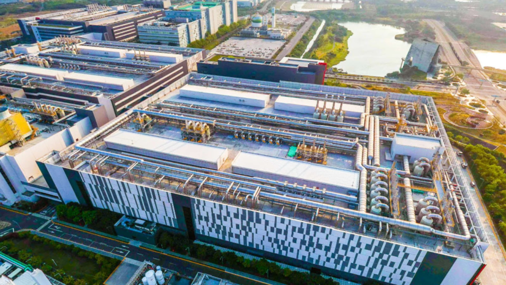
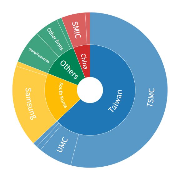
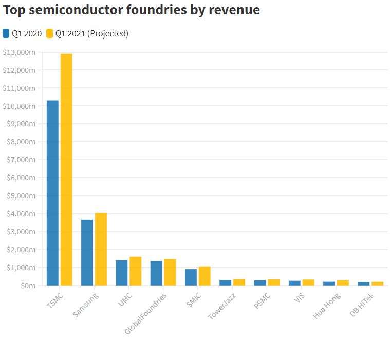
The location to build a fab is dependent on multiple factors: tax incentives, educated workforce around, and especially constant supply of power and water. GlobalFoundries Fab 8 in Luther Forest, Upstate New York is expected to complete its water, sewage & road connections in 2 years from July 2009. It ended up taking 7 years, with $65 million spent on building a 28-mile pipeline and a purification plant on the Hudson River capable of purifying 14 million gallons of water every day. On the other side of the planet, Taiwan is suffering from serious drought since March 2021 and has decided to shut off irrigation across 183,000 acres of farmland to focus its water supply on TSMC fabs. A difficult but reasonable decision considering these foundries are supplying over 92% of chips under 10nm for the whole world, and TSMC needs 156,000 tons of water daily to operate them [3].
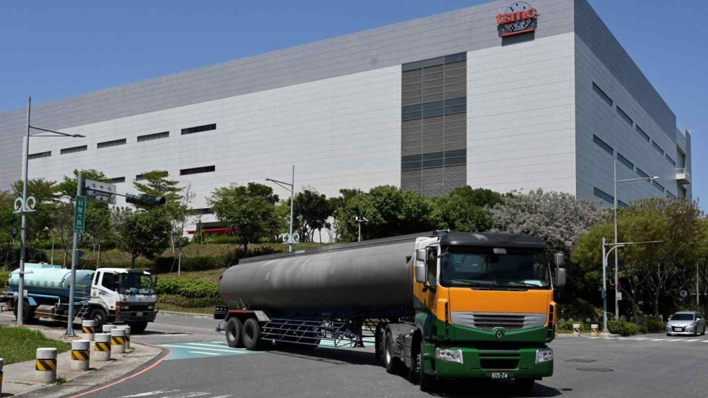
Geographic and geological concerns also play a role in building a fab. The process of manufacturing transistors with a size 10,000 times smaller than the diameter of human hair requires extreme precision. Therefore all vibration from the external environment needs to be eliminated. Taiwan happens to be at a location with very frequent earthquakes, and TSMC had to build dampers into their facility to reduce seismic effects by up to 40%. These infrastructures cost a lot of money, had to be tested and constructed correctly and timely.
Clean Rooms
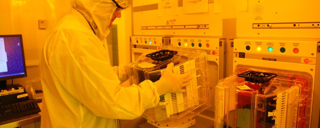
The heart of a semiconductor fab is its clean rooms, where the chip fabrication actually happens. In these rooms, a single particle can become a mountain compare to nano-size transistors, crushing them and destroying the performance of a whole device. Pure air needs to be constantly pumped in a space that spans across 5 soccer fields (TSMC Fab 14 – around 31,000 square meters), and people going in these facilities are all required to suit up. These rooms are also always basking in yellow light because chips are sensitive to UV rays. Clean rooms are classified according to the cleanliness level of the air inside the controlled environment. Class 1 indicates no more than 1000 particles of size larger than 0.1um per cubic meter. Class 10 means no more than 10,000 such particles, Class 100 means no more than 100,000, and so on. If you wonder how clean is that, then every cubic meter of room air contains 35 million particles of size > 0.5um [4].
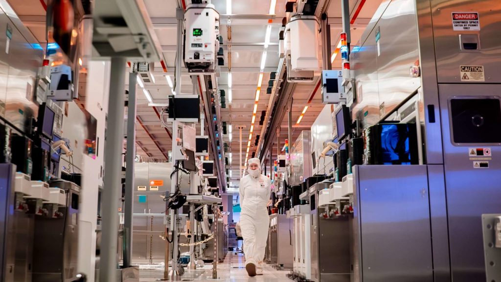
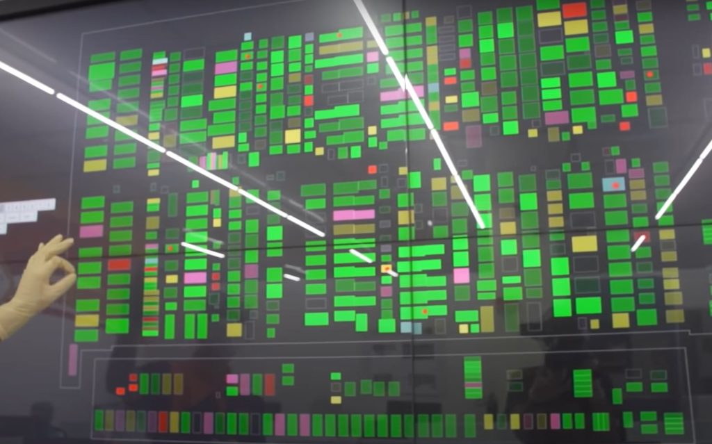
Human is a huge source of particles, and therefore never once during the manufacturing process do the wafers come into contact with any of the worker. Wafers are stored in special containers, each carrier can hold up to 25 wafers, and there are around 4,000 of these moving around on rails on the ceiling of GlobalFoundries Fab 7 in Woodlands, Singapore. Basically, over 95% of the processing jobs are fully automated by machines that are remotely controlled from operation stations.
Machines
The machines inside a fab typically add up to 75% of the total cost of the entire foundry. Engineers, therefore, need to carefully select and acquire the right equipment, make sure they are delivered within budget as well as on time. A cutting-edge EUV machine from ASML can cost over $120 million by itself [5], and the fab must manage to properly bring it over and install it in the cleanrooms, a nerve-wracking task. Many other machines also cost millions of dollars, some are as big as a school bus, and any accident may render them malfunctioned, forcing the fab to return them for calibration, costing hundreds of thousands of dollars and incalculable lost time.
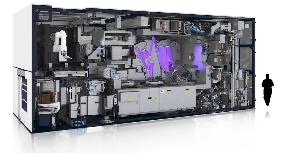
With all the costly investments, people want their fabs to perform at their maximum optimization, sparing no expense. GlobalFoundries said its fab in Singapore typically produces around 600,000 wafers a year, but with the surge in demand, they’re making an additional 120,000. Almost every fab is put into operation long before it has completed all of its infrastructures, a process that will take years to finished. Incredibly precise management and tracking are applied to ensure income can be generated as soon as possible. It’s like sailing out into the ocean and try to assemble your ship along the way, a hard and unforgiving task, where any mistake means millions of dollars wasted.
Conclusion
“The semiconductor is the brain within the head. The software is the wisdom and data is the knowledge.”
Masayoshi Son – Chairman & CEO of Softbank.
Making chips is an exceptionally difficult task, but is also a remarkable feat of human engineering. These chips are the fuel of our lives, the backbone of many industries of the modern world. Thousands of companies are dependent on semiconductor devices, and only several fabs in the world are producing what they need. A huge part of the global economy is now in the hand of certain chipmakers, and even a drought on an East Asian island can send ripples across the world.
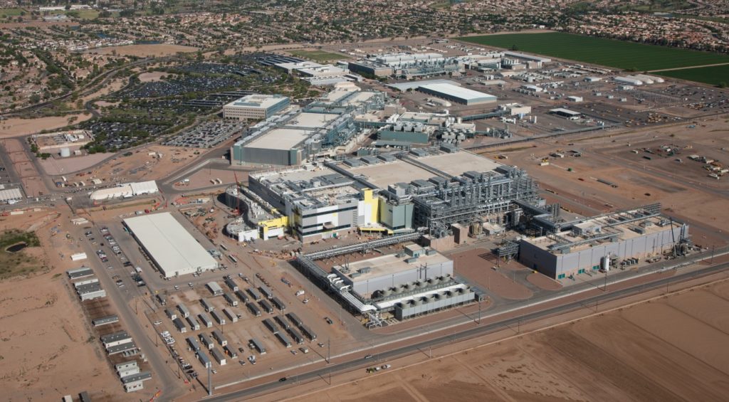
Many plans of building a new fab have been announced, from TSMC ($12 billion in Arizona), Intel ($20 billion in Chandler, Arizona [6]), to Samsung ($18 billion in Austin, Texas [7]) and Bosch (Dresden, Germany [8]). However, building fabs is always extremely challenging, risky, costly, and time-consuming. Rome cannot be built in one day, and neither will these upcoming foundries be completed anytime soon to relieve the world from the crisis of chip supply.
Reference:
- General Motors Says Chip Shortage Likely to Stall 2021 Earnings. The Street. Feb 10, 2021.
- Taiwan chipmaker TSMC’s $12 billion Arizona factory could give the US an edge in manufacturing. Sherisse Pham, CNN Business. May 15, 2020.
- Taiwan cuts water two days a week amid the worst drought in years. Elizabeth Shim, WORLD NEWS. April 16, 2021.
- Cleanroom Classifications. 2021 Clean Air Technology, Inc.
- EUV tool costs hit $120 million. https://www.eetimes.com/. Max LaPedus. Nov 19, 2010.
- Intel is spending $20 billion to build two new chip plants in Arizona. Kif Leswing. Mar 23, 2021
- Samsung Electronics to Build EUV Foundry in Austin. Korea IT News. May 18, 2021.
- Bosch opens wafer fab of the future in Dresden. EP&T Magazine. June 8, 2021.

Usually I don’t read article on blogs, but I would like to say that
this write-up very forced me to take a look at and do it!
Your writing style has been amazed me. Thank you, very
nice article.