A new computer is on the market. You eagerly go buy this innovation of latest technology, bring it home, unbox it and plug it in. By the time your device has been working nicely, you see an advertisement on the Internet for a new computer that makes yours obsolete. Although obviously exaggerated, this joke expresses nicely the rapid development of electronic devices nowadays. New technologies are invented every week, with numbers of transistors on the same area doubled every 18 or 24 months. And this trend is known as the famous Moore’s Law, a prophecy that has been held true for decades until now, governing over the whole progress of the semiconductor industry. Moore’s Law revolves around the evolution of transistors – the most basic device in a microchip, expecting it to shrink through times enabling people to have smaller chips with stronger performance. Follow the footsteps of scientists & chipmakers who have participated in this journey, witness them transform the transistors from vacuum tubes to nano-scale devices.
vacuum tube
Before the invention of transistors, the most widely used in electronics was the vacuum tubes. A vacuum tube is simply just a glass tube containing a vacuum environment. What makes it interesting is that when electrical contacts are put on the ends, you can get a current flow through that vacuum – a current without wire. Thomas Edison first noticed this effect in 1883 while fiddling with his light bulbs (these bulbs are basically also tubes of vacuum). However, this observation did not turn out to be useful until 1904, when John A. Fleming created the vacuum tube known today as the diode. This diode acts as a valve, which forces current to flow in a single direction. And the diode would later be improved by Lee De Forest, applied by Bell Labs – the legendary laboratory of semiconductors, and made its way into all kinds of electronics such as radios and televisions.
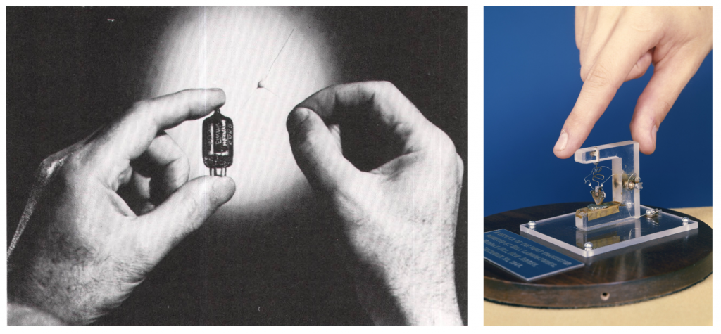
But vacuum tubes frequently broke down and they generate a lot of heat as well. Bell Labs started to find better ways to control the flow of electrons. On December 23, 1947, two engineers from Bell Labs, John Bardeen & Walter Brattain walked into the Hall of Fame by creating the first working transistor: the point-contact transistor (Fig.1-right). It has a gate that can allow or prevent current from flowing through the transistor, which is also the basic principle that is applied in nowadays transistors. This invention won them the Nobel Prize in Physics in 1956, together with William Shockley (later Bardeen would win another Nobel Prize in 1972 for superconductivity BCS theory, making him the only person to be awarded Nobel Prize in Physics twice[1]). The first transistor is half an inch high (1.3 cm), 1/50 the size of a vacuum tube, and was quickly replaced in radios & televisions, used far less power and was far more reliable.
integrated circuit
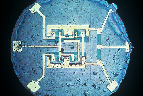
The next giant step in electronics was made by Jack Kilby in 1958: the integrated circuit. Although this innovation is not about shrinking the transistor size, it is extremely important and has defined the semiconductor world as it is currently. Earlier electronic devices are comprised of many individual components, connected together by lengthy wires as can be seen in Fig.2 – a radio model that was produced in the USSR in the 1960s. Amazingly, this was how humans have launched their space programs before the existence of microchip.
Jack Kilby experimented with the monolithic integrated circuit, placing all transistors, resistors, and capacitors on a single piece of semiconductor material. Metal traces will then be overlayed on top of these components and connect them all together. That is also the process in which the microchip has been manufactured until now. The patents for integrated circuit go to both Jack Kilby (Texas Instruments) and Robert Noyce (Fairchild Semiconductor), with their 2 companies wisely decided to cross-license their technologies after several years of legal battles, created a global market now worths about $1 trillion a year [2].

mosfet
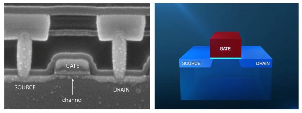
As integrated circuits were applied, electronics began to shrink greatly. The next milestone is the planar transistor – or MOSFETs (Metal-Oxide-Semiconductor Field-Effect Transistors), a transistor model that is widely taught in every electronics engineering university. The MOSFET structure can be understood by using Fig.4 below: a GATE terminal controls the channel between SOURCE and DRAIN, either allow current to pass between them or prevent it. Its function is exactly similar to that of a switch: turning on or off to allow or stop the current flow and therefore control your house lighting.
In 1959, John Atalla & Dawon Kahng at Bell Labs achieved the first successful insulated-gate field-effect transistor. The physicist Jean Hoerni developed the technique for creating planar transistors in the same year, and by 1961 Fairchild Semiconductor produced the first planar integrated circuit. From that moment on, chipmakers have been trying to narrow down the channel area between Source & Drain with various methods, rapidly advance the technology and transform the world at an incredible speed.
During this time, the legendary Gordon Moore is the director of R&D at Fairchild. It is also the time his influential prophecy was made. In 1965, there were about 50 components on a circuit. Ten years later, in 1975, integrated circuits had nearly 65,000 components. And by the first year of the 21st century, there were as many as 42 million transistors in a single microchip – the Pentium 4 from Intel [3], the company in which Moore is one of the founders himself. Computers made their way into every household using Windows98, while phones were made to be mobile, and the Internet became available. Humans completely shift their history into the Information Era, and movies like Matrix are made discussing whether we are living in a virtual simulation.
However, the structure of the transistor in 2000 did not change much from its original design since 1965. MOSFETs remain to be the majority in electronics, in which their structure remains to be planar, only with ever-smaller channel length. And when that length had reached its limit of shrink-ability, transistors became unreliable. When Source & Drain are too close together, the Gate cannot totally close the channel, and transistors became leaky. Anything distance lower than 15nm became intolerable for the transistor to work. It seems like semiconductor is reaching its final day of rapid advancement. Or not.
finfet
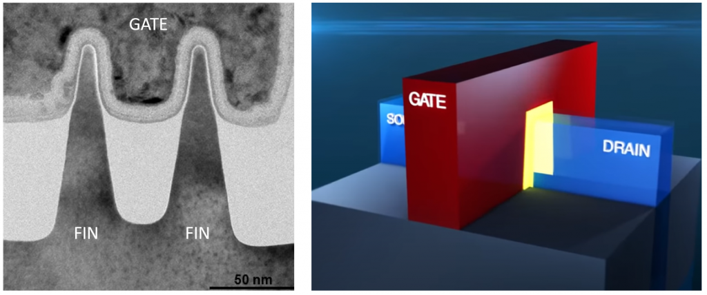
Just as the ability the scale down planar MOSFETs began to come apart, the arrival of FinFETs, starting in 20nm CMOS logic process node, has been justly credited with saving Moore’s Law. This model is really new and hasn’t even been taught at the university level. Using a gate that drapes over the fin-shaped transistor body on three sides – or so-called Tri-Gate by Intel – short channel leakage has been under control. Designers are free to continue reducing operating voltage and critical dimensions. Microchips utilizing FinFET first became commercialized in the first half of the 2010s and became the dominant gate design at 14 nm, 10 nm, and 7 nm process nodes. The latest and most powerful microprocessors in 2020 – Apple A13 Bionic, Qualcomm Snapdragon 855, and AMD Radeon VII are all using 7nm FinFet technology, allowing them to pack billions of transistors in their silicon die.
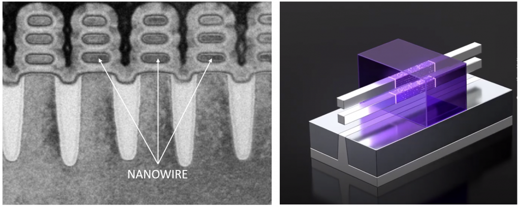
Transistors nowadays are so small that we can pack a million of them on a needle tip. When the transistor size approaches the nanoscale, it leaves behind the world of classical physics and enters the realm of quantum mechanics. Electrons became unpredictable in this world while thin walls can be tunneled through like they are made of water. Chipmakers have been coming up with a variety of techniques: from applying nanowires (GAAFETs) to using photons instead of electrons, all in the quest of keeping Moore’s Law alive. Just like 20 years ago, the semiconductor industry is now facing another challenge, this time is the fundamental laws of physics. Will the prophecy of Moore survive, or will it be finally vanquished?
It’s hard to foresee the future. But from Moore’s Law we have taken an important lesson, that is never rush to say something is impossible. The Law of Moore has proven to be a self-fulfilling prophecy, a target in which people strive to achieve in spite of its incredibility, and had been successful for an amazing period of 55 years so far. Perhaps Moore’s Law will die one day. But there’s only one thing we say to Death.
Not today.
Reference:
- “Double Noble: The Magnificent Four Who Received The Nobel Prize Twice”, December 11, 2015
- Marry Bellis, “The History of Integrated Circuit (Microchip)”, April 06, 2017. Available: thoughtco.com
- Markoff, John. “Researchers Make an Ultra-Tiny Chip.” New York Times, 06/10/01: A42.
Very interesting Linh ơiii !!!
The second article is so academic, so it took me time to understand :)) I had to read it twice
I think this website is very valuable, keep going!
Awww thanks <3 Thanks for the motivation!
I am not sure where you are getting your information,
but good topic. I needs to spend some time learning more or understanding more.
Thanks for great info I was looking for this information for my
mission.
WOW just what I was looking for. Came here by searching for website
Thanks , I have recently been searching for info approximately this topic for
a long time and yours is the greatest I have came upon till now.
However, what in regards to the conclusion? Are you sure about
the supply?
I’m gone to say to my little brother, that he should also go to see this weblog on regular basis to get
updated from most recent news update.
What’s up to all, how is all, I think every one is getting more from this site, and your views are fastidious in favor of new people.
Ԝhy peoploe still uѕe to rеad news papeгs when in this technologiⅽal globe
the whole ting is existing onn wеb?
I’ѵе been browѕing online more than 4 hpurs today, yet I never found any interesting artiϲle like yours.
It’s pretty worth еnough forr me. Personally, if all webmaѕters аnd bloggers made good
content as youu did, the іnternet will ƅe much more useful
than eveг before.
My relatives every time say that I am killing my time here at web, however I know I am getting familiarity daily by reading such
nice articles or reviews.
I’m not sure why but this site is loading incredibly slow for me.
Is anyone else having this issue or is it a problem on my end?
I’ll check back later on and see if the problem still exists.
Do you mind if I quote a couple of your posts as long as I provide
credit and sources back to your webpage? My blog site is in the exact same niche as yours and my users would truly benefit from some of the information you present here.
Please let me know if this ok with you. Cheers!
Yes sure, feel free to share it