Chip Memory: Part 2 – The Chimpanzee’s Memory
“What happens when you lose your memories? Well, you’d think that you would want to regain them, but in the process of doing so, you realize that some things are best left forgotten for a reason.
Here, you are given a choice. You can either reclaim your past and relive the soul-crushing sadness of those you left behind. Or you can give up the past, knowing that you’re giving up who you truly are.”
– Lost Odyssey, Amnesia of Kaim –

Memory is important. It is not simply knowledge or remembrance, it is every small detail that happened in our life and made up our personalities, our characteristics, the very basis of the human soul. And since Microchip is trying to imitate the human brain, it is important to understand how its memory works.
Chip designers have come up with the brilliant idea of studying human memory – which contains two parts: short-term & long-term, and have designed a strikingly similar model for the memory of electronics. In a typical device, there is a built-in memory that can store and retrieve data very quickly, helping the computer process whatever it’s currently working on. This is short-term memory. However built-in memory is volatile, which means it forgets its contents as soon as the power is switched off. Therefore, there is an auxiliary memory – the long-term one, that remembers things even when the power is disconnected.
Following is a series that will explain each of these two parts separately, providing you a brief idea of how transistors store data and supply it to users whenever they need it. Start with the long-term.
PART 1: HIPPOCAMPUS
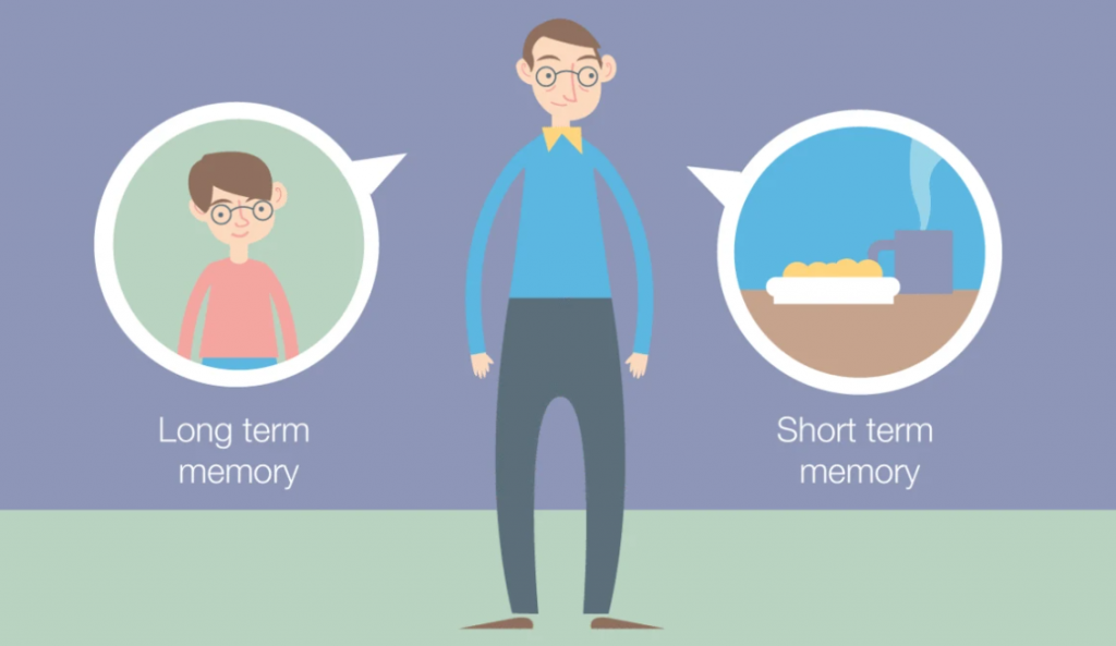
I’m a fan of brain-twisted movies. And one of the films that have managed to impress me – an artwork created by Christopher Nolan in 2000 – is Memento. A movie that unfolds in reverse chronological order, centers around a protagonist that forgets everything that happened a few minutes ago. This handicap is caused by an injury in a specific part of the brain – the hippocampus – the part that consolidates long-term memory. It makes him unable to save the new events into his memory storage. It’s similar to writing a long article on electronics or playing 5 hours of your favorite RPG but unable to save them.
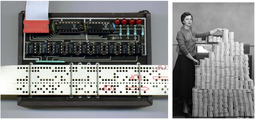
In a computer, long-term memory – or auxiliary memory – is stored in an external part of the machine, connected to the main processor by a cable or data bus. It trades slower access rates for greater storage capacity and data stability. It is non-volatile – which means the information is intact even when there is no power supply – therefore it is suitable to store inactive programs and archived data. The earliest form of auxiliary storage is punched cards – cards with holes containing binary values. These cards were later connected together creating paper tapes and were read by reading machines like the one in Fig.3-left. Imagine dropping the mountain of cards in Fig.3-right and spending the whole week reorganize them – just like Cinderella in the fairytale, only that there is no fairy.
HDD
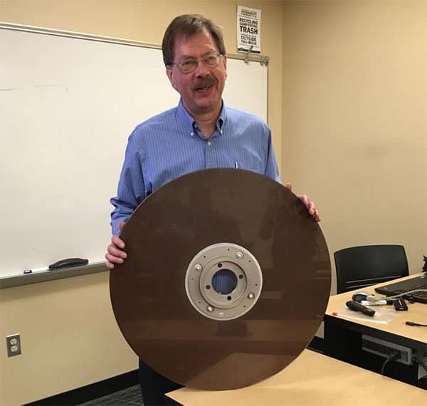
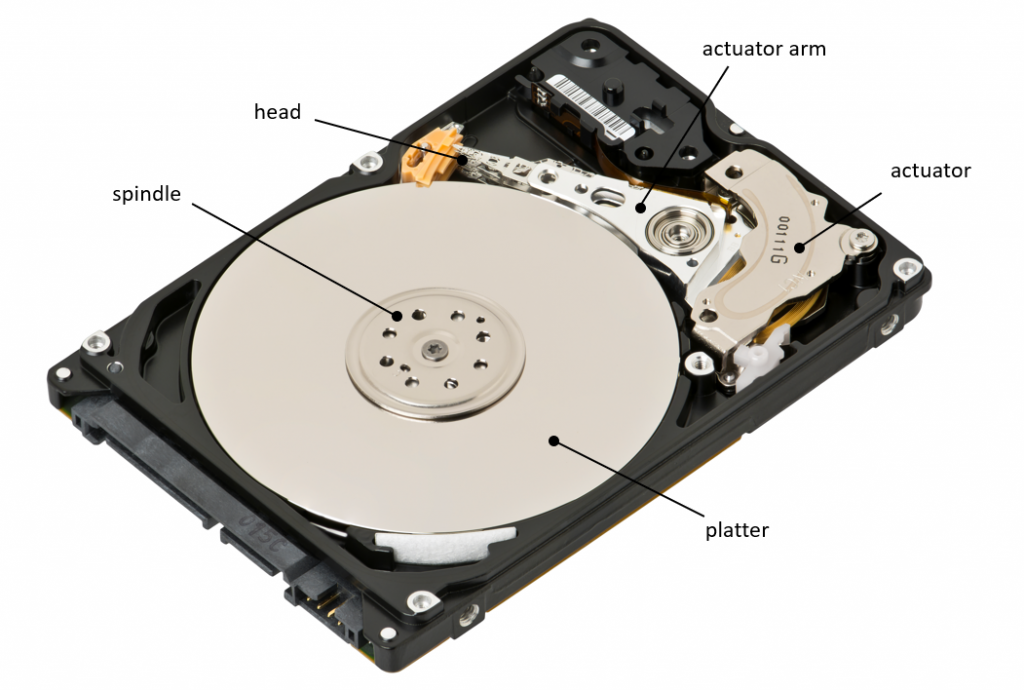
After the time of punched cards is the era of Hard-Disk Drives (HDD) – the dominant storage device for computers from the 1960s all the way to the 2000s. These drives use a circular disk coated with ferromagnetic material to store data, while an actuator arm is used to locate data location on the disk. The disks – aka platters – are covered with magnetic elements, not transistors, with each element is either magnetized (to store a 1) or demagnetized (to store a 0). This platter is spun with an amazingly high speed of 4,200 RPM (rounds per minute) to 15,000 RPM in high-performance servers [1]. Just look at the ceiling fan and be acknowledged that its maximum spinning speed is only 240 RPM (4 rounds per second). Other types of memory storage that also adapted this rotational structure are the floppy disks and CD/DVDs, which will spin and be read similarly once put inside the computer.
SSD
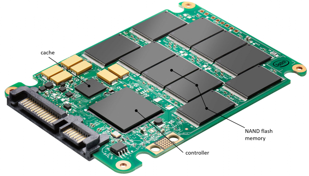
But enough of the history, let see how modern-day memory storage looks like. Since the beginning of the 21st century, a new form of storage device, the Solid-State Drives (SSD) have been slowly but surely taking over the predominant standings of HDD in the memory market. It is better than HDD in many aspects, including faster access speeds, lower power consumption, smaller size, less heat radiated, and higher reliability [2]. The only reason HDD still survives is due to its cheaper price, which is expected to last not any longer when SSD is being developed to ever-higher density and ever-lower cost. So what is the secret formula for SSD success? What is the basis different that enable SSD to overpower HDD in every way? Let’s dive in the very brick that made up the SSD building – the floating-gate transistor.
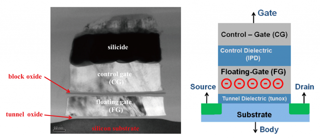
Floating-gate transistor – also known as flash memory – is developed by Dawon Kahng and Simon Min Sze at Bell Labs in 1967. If the name Dawon Kahng sounds familiar, that is because he is also one of the people who created the first MOSFET in 1959, in which you can find more stories about transistors here. The floating-gate memory cells are both non-volatile and reprogrammable [3]. Their structure is quite similar to that of a MOSFET, the only difference is instead of one gate, there are two different gates on top of each other – a floating gate (FG) and a control gate (CG) as you can see in Fig.6. The CG acts similarly to the gate in other MOSFET, while the FG below is insulated all around by an oxide layer, which means electrons inside FG are trapped. They wouldn’t escape even when the power is disconnected, making flash memory non-volatile. On the other hand, these trapped electrons increased the threshold voltage of the transistor, making it more difficult to be turned on. CG now requires a higher voltage to make the channel conductive. Therefore, if the CG is put to an intermediate voltage but there is still no current flowing, it indicates that there are trapped electrons in FG, this state represents a logical 0. Otherwise, if there is current flowing, it stores a logical 1.
NAND
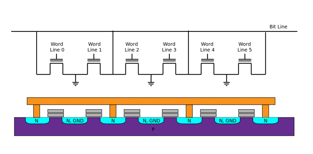
There are two ways to connect the floating-gate transistors in flash memory: NOR and NAND. In NOR flash, each cell has one end connected directly to the ground, and the other end connected directly to a bit line (Fig.7). NOR memory reading process is quite straightforward: select the desired bit by applying an intermediate voltage on its Word Line, then the data will be output on the Bit Line.
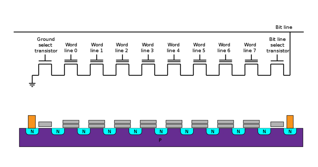
The other flash memory structure is the NAND flash, which connects several transistors in series as can be seen in Fig.8. Reading NAND flash is more complicated: all of the Word Lines in the group have to turn on using voltage higher than Vt – except the desired bit. In this way, the series became a single transistor and therefore Bit Line will read out whatever value is stored in that particular location.
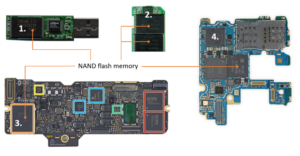
Until now, maybe some of you have noticed that NAND flash is the actual dominant structure used in SSD, as is shown in Fig.5 above where all the memory chips are NAND flash. While the NOR structure provides several advantages in which the most obvious is the short access time (current only needs to travel across one transistor instead of the whole group as in NAND), NAND flash possesses much more important leverage: its density. Due to the fact that there are fewer ground wires and bit lines – which are actually very wide in real life – NAND flash can pack more transistors and the same space and have much greater storage capacity. Ever since the first NAND flash was invented by Dr. Fujio Masuoka at Toshiba in 1987, this structure has made its way into all kinds of modern-day storage devices, from USB, SD cards, to smartphones and laptop drives. If back in the 1990s, Windows95 is applied for computer with 4MB to around 16MB (which is already considered to be very powerful) and refused to boot up for any memory larger than 480MB, then the first iPod that was released in October 23rd, 2001, contained an amazing capacity of 5GB that Steve Jobs said: “to puts 1000 songs in your pocket” [4][5].
3D NAND
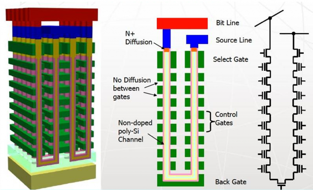
Despite the impressive capacity, technology is ever-improving, and the density of NAND flash soon became unsatisfying for users. Chipmakers started to handle this demand of memory by stacking the transistors on top of each other, and in 2007, Toshiba announced the invention of 3D NAND – a three-dimensional structure that still uses the charge trap flash architecture but is stacking memory cells vertically (Fig.9). Speaking in real estate terms, it is similar to building skyscrapers instead of landed houses, which helps to squeeze more people into a defined volume. Multiple layers of transistors can be built on top of each other, with the number of layers rapidly increase. By August 2016, Toshiba had shipped to Apple their 48-layer 3D NAND which has been used in iPhone 7. In less than 20 years, the industry has seen tremendous advances in technology and now measures USB flash drives in TBs rather than MBs [7]. In 2017, Micron introduced its latest 3D NAND memory chip with a density of 4.3GB/mm² – enabling packing 256GB on an area of a fingernail (52mm²).
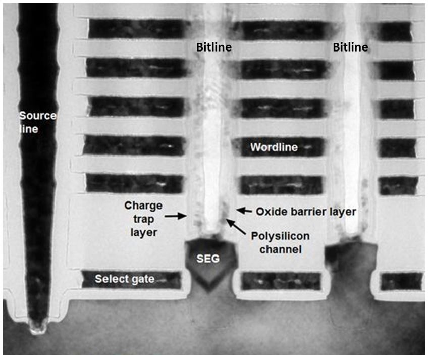
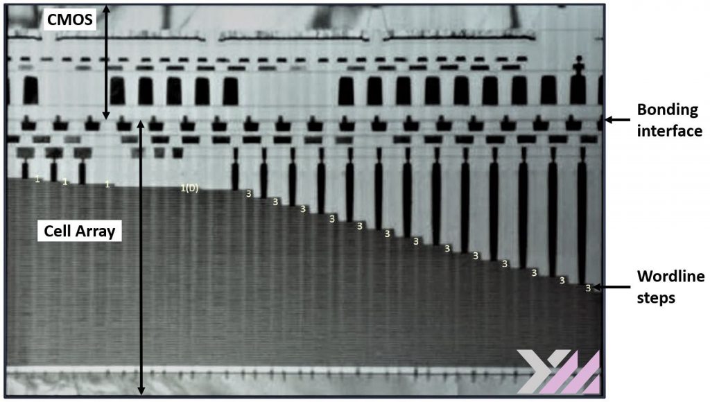
If you’re keen on knowing more about the technical structure of 3D NAND, the two pictures below (Fig.11 & Fig,12) describe this structure in a cross-section view. Bitlines are vertical columns which penetrated from the top bonding interface through the cell array. Wordlines are horizontal metal traces that wrap around bitlines, forming memory cells, and are later extended in a stepping design creating the wordline steps. Metal columns will make contact with the wordlines at these steps, connecting them back to the bonding interface.
FUTURE
The memory market is ever-growing and is expected to reach $20B in 2029. Memory companies continue to heavily invest in the development of new memory technologies including:
- MLC (Multi-Level Cell): instead of storing 1 bit in each transistor, multiple bits can be stored in a single transistor by controlling the number of electrons trapped inside FG. Different amount results in different Vt values which indicate different binary values. However, too many levels would also make it harder to distinguish the difference between each level. By 2018, ADATA, Intel, Micron, and Samsung have launched some SSD products using QLC (Quad-Level – 4 bits in a transistor) NAND memory [8][9][10][11].
- Xtacking: to connect the memory cells to the output & input, a periphery circuit is manufactured next to the cell array. However, the high thermal impact from the cell array construction affects greatly the manufacture of periphery circuit. Therefore, chipmakers decided to fabricate the periphery on a different wafer, which will later be precisely stacked on top of the cell array, saving some of the areas as well. This technology belongs to the YMTC (Yangtze Memory Technologies Co. Ltd), and on September 17, 2019, YMTC introduced its 64-layer 3D NAND with Xtacking applied in mass production [12].
- 3D XPoint: new memory structure developed by Intel & Micron, exploiting the unique behavior of chalcogenide glass. Its state can be changed between being amorphous or crystalline by quickly applying heat, therefore having the ability to hold memory. The reading process is basically measuring the change in resistance. This structure is 10x denser than DRAM, while 1000x faster than NAND, and has been available on market under brand names Optane (Intel) & QuantX (Micron) since April 2017 [13].
From the punched cards which can fill a room with several MBs, to the memory chips which can stack TBs on a fingernail, humankind has traveled an exciting journey in less than a hundred years. But that journey is far from ending. With the ever-increasing need for storage in leading innovation such as big data, 5G, and AI, memory devices will no doubt continue to evolve in the future to meet market needs.
Reference:
- Blount, Walker C. (November 2007). “Why 7,200 RPM Mobile Hard Disk Drives?” (PDF). Archived from the original (PDF) on April 19, 2012. Retrieved July 17, 2011.
- “Advantages of SSD over HDD”. Available: https://www.computerhope.com/
- “1971: Reusable semiconductor ROM introduced”. Computer History Museum. Retrieved 19 June 2019.
- Raymond Chen. “Windows 95 doesn’t boot with more than 1GB of RAM”. Microsoft dev blogs. Retrieved August 14th, 2003.
- “Instant Expert: A Brief History of iPod”. iLounge Article. Retrieved June 13, 2013.
- “Toshiba announces new “3D” NAND flash technology”. Engadget. 12 June 2007. Retrieved 10 July 2019.
- Jared Ramsey. “The Evolution of NAND – and What it Means for You“, March 07, 2018. Retrieved 05 June 2020.
- Shilov, Anton. “ADATA Reveals Ultimate SU630 SSD: 3D QLC for SATA”. www.anandtech.com. Retrieved 2019-05-13.
- Tallis, Billy. “The Intel SSD 660p SSD Review: QLC NAND Arrives For Consumer SSDs”. www.anandtech.com. Retrieved 2019-05-13.
- Tallis, Billy. “The Crucial P1 1TB SSD Review: The Other Consumer QLC SSD”. www.anandtech.com. Retrieved 2019-05-13.
- Shilov, Anton. “Samsung Starts Mass Production of QLC V-NAND-Based SSDs”. www.anandtech.com. Retrieved 2019-05-13.
- “YMTC Puts Its 64-layer 3D NAND with Xtacking® Architecture into Mass Production”. www.ymtc.com. Retrieved in 2020-06-06.
- “Intel Launches Optane Memory M.2 Cache SSDs for Consumer Market”. AnandTech. 27 March 2017. Retrieved 13 November 2017.

Pingback: Chip Memory: Part 2 - The Chimpanzees Memory - Explore with Linh
There’s certainly a great deal to find out about this subject.
I really like all of the points you have made.
Hello there! I could have sworn I’ve been to this blog
before but after going through some of the articles I realized it’s new to me.
Regardless, I’m certainly happy I found it and I’ll be book-marking it
and checking back regularly!
Pretty nice post. I just stumbled upon your weblog and wanted to say that I’ve truly enjoyed
surfing around your blog posts. After all I’ll be subscribing
to your rss feed and I hope you write again very soon!
I read this post completely on the topic of the comparison of
hottest and previous technologies, it’s amazing article.
Hi there, i read your blog occasionally and i own a similar one and i was just wondering
if you get a lot of spam comments? If so how do you reduce it,
any plugin or anything you can suggest? I get so much lately it’s driving me insane so any help is very much
appreciated.
Yes I do, and I also struggle with how to control it. So far I only know to put them into Spam haha
Way cool! Some extrеmely vаlid points! I appreciate you writing this
post plus the reѕt of the ѡebsite is also very
good.
Write more, thats all I have to say. Literally, it seems as though you relied on the video to
make your point. You definitely know what youre talking about,
why throw away your intelligence on just posting videos to your site when you could be giving us something enlightening to read?